


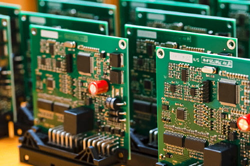
Printed circuit board (PCB) is the support body of electronic components and the provider of circuit connections for electronic components. According to the circuit design, the electrical wiring connecting the electronic components is drawn into a pattern, and then the circuit board is made into a circuit board using the mechanical processing, surface treatment, etc. specified in the design to achieve the purpose of signal transmission and processing.
Printed circuit boards are widely used in various electronic products. Whether in mobile phones, computers, electric vehicles, or smart home appliances, PCB is an indispensable part. It can be said to be a component that is inseparable from modern life. Therefore, there is the "electronics industry mother." In the PCB manufacturing process, it is necessary to ensure the purity of the raw liquid, the acid and alkali liquid used in the process, and the safe disposal of waste liquid. Therefore, in the PCB industry, only by using reliable quality chemical pumps to transport fluids can there be no safety concerns.
The PCB manufacturing process contains many complex stages, some of which require the use of chemical solutions such as etching, development, film stripping, etc. Kung Hai's PTCXPUMP acid and alkali-resistant pumps are suitable for chemical solutions in the PCB industry. For fluid transportation, we can provide pumps that meet the needs of users for acid and alkali fluids or high and low-temperature fluid characteristics.
PCB Process Type:
The printed circuit board process is basically divided into dry process and wet process.
Dry Process:
Cutting → Lamination → Exposure → Lamination → Drilling → Forming.
Wet Process:
Brushing → Inner layer development → Inner layer etching → Inner layer removal → Oxidation → Through hole plating → Full plate copper plating → Outer layer development → Line copper plating → Tin plating → Outer layer removal → Outer layer etching → Film removal → Solder mask printing → text printing → surface treatment.
Next, several important process stages of the wet process are explained below.
1. Brushing
The initial brushing process requires multiple steps of water washing and pickling to achieve the purpose of cleaning.
Water Washing: Wash off the dust on the copper surface to ensure that the surface is clean and dust-free.
Pickling: Clean the copper surface with chemical liquid to increase the roughness and facilitate the subsequent attachment of nickel alloy to the copper surface.
2. Developing
Use the developer to dissolve and rinse the dry film that has not been exposed to light. The dry film after exposure will harden due to exposure to light, so the developer cannot dissolve it and will remain and adhere to the board surface. Form a line pattern.
3. Etching
First use a film remover to wash away the unsensitized outer dry film. The copper surface not covered by tin below (that is, the unnecessary copper surface) will be exposed, and then use etching The liquid is etched to dissolve the copper surface that does not need to be retained. Only the copper surface attached to the dry film will be left to form the circuit area.
4. Plated Through Hole (PTH)
Multilayer PCB is made up of layers of copper foil circuits. Each layer of circuits is connected by via holes, which means drilling Holes are used to connect different circuit layers. However, it cannot conduct electricity simply after drilling. The surface of the through hole must be plated with copper as a conductive substance to allow these circuit layers to be electrically connected.
5. Tin plating (Immersion Tin)
Deposits a thin layer of tin on the copper surface of the PCB. Its function is to protect the copper surface from oxidation before etching.
6. Stripping
Use tin-lead stripping liquid to wash away the tin on the surface, leaving the required circuit pattern.
7. Surface Finish
Finally, surface treatment is performed on the exposed copper surface that is not covered by the solder mask layer to avoid oxidation of the bottom copper surface to ensure good solderability during the PCB assembly process. or electrical conductivity performance.
There are two common types of surface treatment technologies: metal and organic. HASL, immersion gold and immersion tin all belong to metal surface molding, while OSP belongs to organic surface molding.
After the circuit board is manufactured, it is crucial to correctly handle the waste liquid at the end of the process and effectively prevent pollution problems. It is crucial to establish a complete recycling and emission system, so as to take into account both safety and environmental protection.
PTCXPUMP Sealless Magnetic Pump Can Be Safely Used In:
- Chemical supply equipment
- Internal process supply system
- Waste liquid treatment equipment
PTCXPUMP sealless magnetic pump provides you with the best solution for conveying fluids in PCB industry applications. The sealless design can effectively avoid leakage, and the material used is GFR-PP and CFR-ETFE, which has excellent corrosion resistance and is suitable for transporting highly corrosive or flammable or explosive high-risk fluids such as acid and alkali liquids. In the PTCXPUMP sealless magnetic pump series, PTC-100 ~ PTC-251 are for small applications, and PTC-400 ~ PTC-675 are for medium and large applications. There are various models to meet your various operational needs. PTCXPUMP is committed to becoming your first choice for safe use of pumps.

The best solution for chemical fluid transportation》PTCXPUMP sealless magnetic pump / INNOMAG Lined Sealless Magnetic Pump
